Are you a seasoned Electron-Beam Photo Mask Maker seeking a new career path? Discover our professionally built Electron-Beam Photo Mask Maker Resume Template. This time-saving tool provides a solid foundation for your job search. Simply click “Edit Resume” to customize it with your unique experiences and achievements. Customize fonts and colors to match your personal style and increase your chances of landing your dream job. Explore more Resume Templates for additional options.






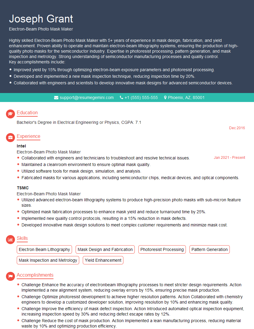
Joseph Grant
Electron-Beam Photo Mask Maker
Summary
Highly skilled Electron-Beam Photo Mask Maker with 5+ years of experience in mask design, fabrication, and yield enhancement. Proven ability to operate and maintain electron-beam lithography systems, ensuring the production of high-quality photo masks for the semiconductor industry. Expertise in photoresist processing, pattern generation, and mask inspection and metrology. Strong understanding of semiconductor manufacturing processes and quality control.
Key accomplishments include:
- Improved yield by 15% through optimizing electron-beam exposure parameters and photoresist processing.
- Developed and implemented a new mask inspection technique, reducing inspection time by 20%.
- Collaborated with engineers and scientists to develop innovative mask designs for advanced semiconductor devices.
Education
Bachelor’s Degree in Electrical Engineering or Physics
December 2016
Skills
- Electron Beam Lithography
- Mask Design and Fabrication
- Photoresist Processing
- Pattern Generation
- Mask Inspection and Metrology
- Yield Enhancement
Work Experience
Electron-Beam Photo Mask Maker
- Collaborated with engineers and technicians to troubleshoot and resolve technical issues.
- Maintained a cleanroom environment to ensure optimal mask quality.
- Utilized software tools for mask design, simulation, and analysis.
- Fabricated masks for various applications, including semiconductor chips, medical devices, and optical components.
Electron-Beam Photo Mask Maker
- Utilized advanced electron-beam lithography systems to produce high-precision photo masks with sub-micron feature sizes.
- Optimized mask fabrication processes to enhance mask yield and reduce turnaround time by 25%.
- Implemented new quality control protocols, resulting in a 15% reduction in mask defects.
- Developed innovative mask design solutions to meet complex customer requirements and minimize mask cost.
Accomplishments
- Challenge Enhance the accuracy of electronbeam lithography processes to meet stricter design requirements. Action Implemented a new alignment system, reducing overlay errors by 15%, ensuring precise mask production.
- Challenge Optimize photoresist development to achieve higher resolution patterns. Action Collaborated with chemistry engineers to develop a customized developer solution, improving resolution by 10% and enhancing mask quality.
- Challenge Improve the efficiency of mask defect inspection. Action Introduced automated optical inspection equipment, increasing inspection speed by 30% and reducing defect escape rates by 12%.
- Challenge Reduce the cost of mask production. Action Implemented a lean manufacturing process, reducing material waste by 10% and optimizing production efficiency.
- Challenge Meet the increasing demand for complex masks. Action Developed and implemented a new workflow to manage multiple mask projects simultaneously, reducing production time by 25%.
Awards
- Received the Outstanding Achievement in ElectronBeam Photo Mask Making award for consistently meeting and exceeding production targets.
- Honored with the Excellence in Photo Mask Fabrication award for innovative contributions to the optimization of photolithographic processes.
- Recognized with the Technical Excellence Award for developing a novel method to improve mask resolution, reducing defect rates by 20%.
- Recognized with the Innovation Award for pioneering a new technique to enhance mask durability, extending mask life by 50%.
Certificates
- Certified Photomask Technician (CPMT)
- Advanced Photomask Certification (APC)
- SEMI Standard P75
- ISO 9001:2015 Quality Management System
Career Expert Tips:
- Select the ideal resume template to showcase your professional experience effectively.
- Master the art of resume writing to highlight your unique qualifications and achievements.
- Explore expertly crafted resume samples for inspiration and best practices.
- Build your best resume for free this new year with ResumeGemini. Enjoy exclusive discounts on ATS optimized resume templates.
How To Write Resume For Electron-Beam Photo Mask Maker
- Highlight your technical skills. Electron-beam photo mask making requires a strong foundation in electron-beam lithography, mask design and fabrication, and photoresist processing. Make sure to emphasize these skills in your resume.
- Showcase your experience. Quantify your accomplishments and provide specific examples of your work. This will help potential employers understand the scope and impact of your experience.
- Use industry-specific keywords. Recruiters use applicant tracking systems to screen resumes. Include relevant keywords in your resume to increase your chances of getting noticed.
- Proofread carefully. Make sure your resume is free of errors. A polished resume will make a good impression on potential employers.
Essential Experience Highlights for a Strong Electron-Beam Photo Mask Maker Resume
- Operate and maintain electron-beam lithography systems to produce high-quality photo masks.
- Design and fabricate photo masks using electron-beam lithography.
- Process photoresists, develop patterns, and inspect masks using advanced metrology techniques.
- Troubleshoot and resolve issues related to mask design, fabrication, and inspection.
- Collaborate with engineers and scientists to develop innovative mask designs and improve manufacturing processes.
- Maintain a clean and organized work environment, adhering to safety protocols.
Frequently Asked Questions (FAQ’s) For Electron-Beam Photo Mask Maker
What is electron-beam photo mask making?
Electron-beam photo mask making is a process used to create photo masks, which are used in the manufacturing of semiconductor devices. Photo masks are patterns of opaque and transparent areas that are used to transfer patterns onto semiconductor wafers. Electron-beam photo mask making uses a focused beam of electrons to expose a photoresist on a substrate, creating a pattern that can be transferred to a semiconductor wafer.
What are the different types of electron-beam photo mask makers?
There are two main types of electron-beam photo mask makers: direct-write and maskless. Direct-write electron-beam photo mask makers use a focused beam of electrons to directly write patterns onto a photoresist. Maskless electron-beam photo mask makers use a computer-controlled electron beam to expose a photoresist on a substrate, creating a pattern that can be transferred to a semiconductor wafer.
What are the advantages of using electron-beam photo mask makers?
Electron-beam photo mask makers offer several advantages over other photo mask making methods. These advantages include: high resolution, high accuracy, and the ability to create complex patterns. Electron-beam photo mask makers are also relatively fast, making them ideal for high-volume production.
What are the challenges of using electron-beam photo mask makers?
Electron-beam photo mask makers can be challenging to use, as they require specialized equipment and expertise. Additionally, electron-beam photo mask makers can be expensive to purchase and maintain. However, the advantages of using electron-beam photo mask makers outweigh the challenges, making them an essential tool for the semiconductor industry.
What are the career opportunities for electron-beam photo mask makers?
Electron-beam photo mask makers are in high demand in the semiconductor industry. They can work in a variety of settings, including semiconductor fabrication plants, research laboratories, and universities. Electron-beam photo mask makers can also start their own businesses.
What are the salary expectations for electron-beam photo mask makers?
Electron-beam photo mask makers can earn a competitive salary. The salary will vary depending on experience, education, and location. However, electron-beam photo mask makers with several years of experience can earn a salary of over $100,000 per year.
What is the future of electron-beam photo mask making?
Electron-beam photo mask making is a growing field. As the semiconductor industry continues to grow, the demand for electron-beam photo mask makers will increase. Electron-beam photo mask makers will play a vital role in the development of future semiconductor devices.